
Have you ever asked yourself a seemingly trivial question: why does a CPU have cache levels at all, if you could just take one big cache instead? The answer to this question is tightly interwoven with semiconductor physics, the history of processor architecture, and the way compilers learned to make use of the memory hierarchy.
The first thing to understand: a processor isn't an abstract calculator, it's a very real piece of silicon roughly the size of a thumbnail, holding billions of transistors. When we say “data is transferred from memory into a register,” we literally mean that an electrical signal travels along a metal wire a few millimeters or centimeters long. That, too, is a distance — negligible by human standards, but at a clock frequency of 3–4 GHz it already matters, simply because in one cycle a signal travels at best around 10 centimeters in ideal conditions, and even less along a metal wire on the die.
In other words, the path of a signal along a wire between two points on the chip is not an instant teleportation of data, because it's a physical medium with delay, resistance, and power consumption proportional to length — and it's exactly this physical limitation that makes a single large cache impossible: the farther a memory cell sits from the core, the longer you have to wait for an answer.
Physics dictates the architecture
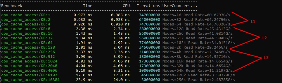
If you took the entire cache of a modern CPU, something around 2 MB, and turned it into one big storeroom, the core would have to walk over there on every access and wait for the signal to travel, possibly to the farthest corner, and come back. And the bigger the cache, the more complex its addressing logic, the more energy is spent on every access, and the worse the density. Fast L1 SRAM cells take up far more area than all of the slow L2, so chip designers eventually arrived at a natural hierarchy: a small, fast cache right next to the core, then a bigger and slower one further out, and an even bigger and even slower one beyond that.
To feel the logic of the hierarchy not in the abstract but through a clear example, imagine you're decorating a Christmas tree on a December evening, hanging ornaments on it. In your hands you have a small box holding five or six ornaments you just picked out, and grabbing any one of them takes a couple of seconds — that's our L1 cache, right at hand.
Next to you on a chair sits a cardboard box where you dumped ornaments from your stash the day before, and to get something out of it you have to reach over, dig around a bit, find the right shape or color. All of that takes more time — and that's the L2 cache: noticeably bigger, a bit slower, but still within reach from the same spot.
But the box isn't bottomless either, and at some point it runs out of the type of ornament you need, and then you have to go to the next room, where the big bag with the main stash sits. That is, you have to get up, walk out, dig through the bag, find what you want, and come back — a break in the not-so-simple business of decorating the tree, and it takes a noticeable amount of time. This is our L3 cache, with a large capacity, access to which requires effort and time, but where almost everything is.
And finally, up in the attic stands an old chest of drawers holding Christmas ornaments going back to Soviet times: rare, interesting, but getting to them amounts to an expedition — you have to find a ladder, climb up, and search for something among that clutter. While you do that, work at the tree comes to a complete halt — this is the analog of RAM, with enormous capacity, but the latency is so great that in that time you could have hung a dozen ornaments. Sound familiar?
And notice that while I was telling this analogy, it never occurred to you to remove all four storage spots and replace them with one giant shelving unit right there in the room. Formally that would be “everything in one place,” but the box in your hands abruptly stops being the box in your hands and turns into one corner of a huge rack you still have to reach for, and the entire benefit of “at hand” disappears. That's exactly why you can't just take 32 KB + 256 KB + 2 MB and stack them into one L1 — because a physically large cache cannot be physically fast.
Historical context
The cache hierarchy in processors didn't appear all at once, and the history of its development illustrates well how much this decision was dictated by physical and economic constraints rather than theoretical considerations. The first processors of the late 1970s had no hardware cache at all and worked directly with external memory, and latencies were comparable to a single cycle, so there was almost no gap and the problem was imperceptible.
When, in the early 1980s, processors started getting faster than memory, manufacturers added a small cache, first on the board and then on the die. In 1989 the i486 came out, becoming the first mass-market processor with an on-die L1 cache, unified for instructions and data. And around the same time compilers (first of all Borland C++) began applying the notion of data locality, optimizing the placement of variables and the order of declarations in structures and trying to lay hot fields next to each other — although compilers had no formal cache model yet, and all of it was done empirically.
Pentium in 1993 split the cache in two (for data and for instructions), because the different physical requirements of the two traffic types finally got reflected in hardware. Compilers gradually accounted for this too, and binaries started separating code and data sections more carefully, while GCC gained function alignment optimizations to improve instruction-cache hit rates. With the Pentium Pro in 1995, the L2 cache was moved to a separate chip for the first time, and the hierarchy became explicit and two-level. And by the Nehalem era (2008) the familiar three-level scheme had taken shape, with separate L1I and L1D, a unified per-core L2, and a shared L3.
LLVM, which appeared right in this period, absorbed the prior knowledge and was designed from the start with this hierarchy in mind, including passes for loop tiling, prefetching, and hot data layout.
Different kinds of accesses need different structures
People often miss that L1D (the data cache) and L1I (the instruction cache) are fundamentally different devices with different requirements, and that's exactly why they can't be merged into one even at the same capacity. L1D reads and writes individual elements from 1 to 8 bytes in size and must support several read and write ports simultaneously, handle store forwarding, and track coherence with other cores. L1I, from the core's side, is strictly read-only, which lets you greatly simplify its logic, but in exchange it has to provide enormous bandwidth — for example, Intel Core i7 chips fetching from L1I can read 16 bytes every cycle, which at 3 GHz gives on the order of 50 GB/s for instructions alone. If you add peak instruction traffic and peak data traffic together, the requirements for a unified cache turn out to be mutually exclusive, and trying to build a universal cache for both jobs would mean making both worse.
Another fundamental reason to have separate cache levels lies in separating private and shared space. Going back to the tree analogy: the box in your hands is exclusively yours, and nobody else (except your wife — kidding) reaches into it, and that's exactly why you can work with it without any conditions. L1D is private and lets the core just read and write without any coordination, and it's this privacy that gives that single-cycle access so important for the pipeline. L1I is private for obvious reasons.
L2 is also private, but it already takes on some of the bus traffic and interaction with other cores, which of course affects its speed. L3, on the other hand, is a physically shared resource, like the bag of ornaments that in principle every member of the family can use, and that's exactly why access to it requires coordination through a coherence protocol (MSI, MESI, MESIF, MOESI, MOSI, MOESIF, STANFORD DASH, SGIODP); the bet here is that the two previous levels have already cut the number of accesses enough that coordination doesn't become the bottleneck.
Who are all these people?
MSI is one of the earliest cache coherence protocols. It uses three states: Modified, Shared, and Invalid. When a processor modifies data, the line transitions to the Modified state and all other copies in caches become Invalid; if data is read by several cores, the line is in the Shared state.
The problem with MSI is that it has no Exclusive state, so even if a line is used by only one core, the system doesn't know it, and as a result extra bus operations occur on the transition to a write, increasing traffic and reducing performance.
MESI extends MSI by adding the Exclusive state. If a cache line is present in only one cache and matches memory, it gets the Exclusive state, and this lets the processor transition to a write without additional synchronization with other caches.
MESI's drawback shows up in systems with many cores: when data is shared, lines often move between the Shared and Modified states, causing extra bus traffic and cache line bouncing.
MOESI adds the Owned state to MESI and lets one cache hold a modified line and share it with other caches at the same time without immediately writing to main memory. Other caches can read this line in the Shared state, while the owner remains responsible for the updated data.
MOESI's drawback is more complex state-management logic, and supporting the Owned state complicates the hardware implementation and can increase latency in systems where writes to memory happen often.
MESIF is based on MESI and adds the Forward state: when several caches hold the same line, one of them is designated Forward and is responsible for passing the data to other cores on a read, which prevents the situation where several caches try to answer one request at once.
The protocol's drawback shows up in systems with intensive writes: when data changes frequently, the Forward state brings no significant benefit, while the extra states increase implementation complexity.
MOSI is a simplified version of MOESI without the Exclusive state, but using the Modified, Owned, Shared, and Invalid states with the ability to share a modified line through the Owned state, which reduces the number of writes to memory.
The drawback is the absence of the Exclusive state: even if a line is used by only one core, the system can't optimize the transition to a write, which leads to additional coherence traffic.
MOESIF combines the ideas of the MOESI and MESIF protocols and contains the Modified, Owned, Exclusive, Shared, Invalid, and Forward states, which lets it simultaneously optimize data transfer between caches and share modified lines without immediately writing to memory.
The drawback is the high implementation complexity with a large number of states, which increases the complexity of the hardware logic and can lead to additional latency on transitions between states.
Stanford DASH is one of the coherence protocols, and unlike MESI, where all processors snoop a shared bus, here a special table is used that stores information about which caches hold a specific memory line. When a processor wants to read or modify a line, it consults the table for which processors have copies of the line and sends them messages, which lets the system scale to dozens and hundreds of processors without overloading the shared bus.
The drawback of this approach is the extra memory and latency associated with storing and updating the table, and each access may require additional network messages, which increases overall time compared to simple protocols in small systems.
The SGI Origin Directory Protocol (ODP) was used in the SGI Origin 2000 multiprocessor systems, where information about cache-line owners is stored in a distributed table bound to memory nodes. When a processor modifies data, it tracks all caches holding copies of the line and broadcasts invalidation messages, which lets the system scale efficiently to a large number of processors and memory nodes.
The drawback is the implementation complexity and the high cost of message exchange between nodes, and access to remote memory can have significantly higher latency, while directory messages can create additional load on the interconnect between nodes.
How this affects programming
All of this would be of merely theoretical interest if it didn't directly affect how code is written and compiled, because code that processes data sequentially and predictably runs several times faster than code doing the same thing chaotically. The classic example here is traversing a two-dimensional array: if the outer loop goes over rows and the inner over columns, data lands in the cache one line at a time for several iterations; if you swap the loops around, every access to a new element is a cache miss and a trip to L3 or DRAM for a large array. The performance difference on real tasks like matrix multiplication or sorting can reach ten times or more, and that's exactly why compilers learned to do loop interchange, loop tiling, and prefetch insertion automatically. If you want more technical detail, head over here: Cache pollution? Stock up on tests
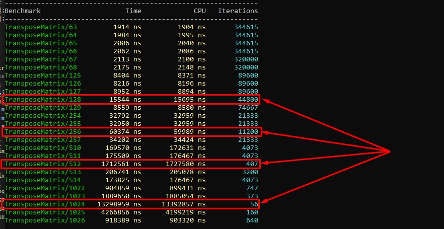
The famous split between AoS (Array of Structures) and SoA (Structure of Arrays) is also a direct consequence of the fact that the L1 cache works in 64-byte lines: if you process only one field of an object while the object itself weighs 128 bytes, you load useless ballast into the cache and halve the effective cache capacity for the current logic.
But do we need an L4 cache?
If the logic of the hierarchy is that each new level brings a gain through larger capacity at an acceptable latency, then a reasonable question arises: “why did we stop at three levels and not add a fourth?” The answer, as always, lies in processor physics, the economics of development, and real usage patterns — and, interestingly, an L4 cache already exists in some systems, we just don't call it that.
Going back to the tree analogy: imagine you placed one more intermediate box between the attic and the next room with the bag. Formally that could speed up access to part of the ornaments from the chest of drawers — if we had to go to the attic often, it would be enough to grab a set of ornaments on the way back and then just glance into the hallway box.
But, as I already said, the gain is noticeable only if we really do have to go to the attic often — that is, if our working set is large enough not to fit in the bag but is still needed often enough for the hallway box to be justified. If, however, we take something new from the attic every time, the hallway box just adds extra shuffling without any speedup, while adding time spent on it and additional problems.
This very consideration determines the fate of the L4 cache in real processors: it makes sense only when a program's working set systematically exceeds L3 capacity while still being hot enough that DRAM accesses become the bottleneck. Such a memory-access pattern is a fairly specific scenario, typical of server databases, large telemetry workloads, and some graphics applications like movie renderers. For a typical desktop application, an L3 of 8–32 MB more than covers most working sets, and adding another level simply won't deliver a noticeable gain.
Nonetheless such applications sometimes creep into ordinary development, and for them there have already been several attempts to build a full-fledged L4 cache. The best-known example was Intel Haswell-GT3e with its eDRAM, released in 2013–2014. There a separate 128 MB eDRAM die was placed on the package next to the processor die, acting as a shared fourth-level cache for the CPU and the integrated GPU at once. The eDRAM latency was higher than that of SRAM caches, but several times lower than that of ordinary DDR3/DDR4, and for graphics tasks like movie editing and heavy rendering, where the working set of textures easily exceeded tens of megabytes, the gain was tangible — on the order of 2x–3x for re-editing movies, which in time terms turned processing a 2-hour film from 12–14 hours into just a few hours.
The compiler, meanwhile, knew nothing about this level and it was fully transparent to software, with the hardware prefetcher deciding for itself what to put there. Intel kept experimenting with this idea in the Iris Pro line all the way up to Kaby Lake, but ultimately dropped it, because the manufacturing complexity and cost of such a processor made it a very niche solution.
In parallel, a similar approach was developing in the world of HBM (High Bandwidth Memory). The idea of memory with a very wide bus, which AMD and Intel began integrating into high-performance GPUs and server processors, is essentially an additional SRAM die next to the ordinary cache — and that's, in effect, a hardware L4, although AMD positions it as an extended L3. The gain for server workloads turned out to be significant, up to 50% performance improvement in certain server tasks, so the technology became standard for the server segment.
As for compilers, explicit L4 support never appeared in them, and they all operate on the model “hot data should fit in the cache” without specifying a concrete level (that's a separate story, because being able to specify the desired storage level would free up to 20% of performance in games), while automatic optimizations like loop tiling are parameterized by cache-line size and approximate level sizes through various flags like -mtune=skylake, but not through an explicit level model. Finer control — when we ourselves plan the placement of hot data structures in huge pages, explicit prefetch hints via __builtin_prefetch or __mmprefetch — also remains the domain of manual optimization in performance-critical cases.
Thus the L4 cache is no longer science fiction, nor even the future, but quite a reality in niche scenarios — yet you shouldn't expect it to appear en masse in desktop processors. Because each new level of the hierarchy adds coherence complexity, manufacturing cost, and specialized management logic that are justified only when the workload profile demands it. The hallway box between the bag and the attic really does help, but only if you live next to the attic and go up there often.

Surely we definitely don't need L5?
L5 in the CPU cache hierarchy doesn't appear anywhere as a production solution as a separate level, but that doesn't mean the idea of five levels is impossible — it just runs into several walls at once.
Each new level of the hierarchy requires solving two problems at once: it must be fast enough relative to DRAM to justify its existence, and cheap enough relative to the previous level in die area or manufacturing cost to make any sense at all. With L4 this still works out, and the same eDRAM and HBM give 3–5 times lower latency than DDR5 at a reasonable cost, but L5 ends up in a situation where there's no longer enough of a gap between it and L4 — neither in speed nor in density — to insert something fundamentally new there.
The coherence problem also grows nonlinearly: each new level shared between cores requires complicating the MESI/MOESI protocol, adds new classes of races, and increases the agreement time, creating new classes of conflicts on invalidation. Three levels are already a complex engineering system, four spills into niche solutions for specific workloads, and five is essentially the point where management complexity probably starts eating up the entire potential gain.
But it's not all so clear-cut, and instead of adding yet another cache level the industry went down other paths that fulfill the same function in spirit but are called something else. As I already wrote, AMD 3D V-Cache is formally positioned as an extended L3, but physically it's a separate SRAM die stacked on top of the compute chip, and in some architectural models it can well be considered L4. Intel, on the other hand, introduces the notion of a “High Bandwidth Cache” or “Memory-side Cache,” deliberately moving away from numbering — and in server systems such an entity effectively plays the role of “L5” in terms of latency: it's faster than disk but several times slower than local DRAM, except this is no longer a cache in the hardware sense, just a different region of the address space with different latencies.
Speculating, the only realistic scenario for L5 would be systems with very heterogeneous memory: for example, future chips with several levels of 3D memory, where you could build a chain like “SRAM → EDRAM → HBM → L5? → DDR → NVM.” Research projects in the academic literature describe such schemes, and IBM in its z-series mainframes has historically used nonstandard memory hierarchies with more levels than is customary in the x86 world, but for the mass market this remains an area of architectural research rather than production solutions for now. Going back to the tree analogy — nobody has yet figured out what to put between the attic and the chest of drawers so that it would be faster than the chest, cheaper than the attic, and large enough to make any sense at all.
← All articles